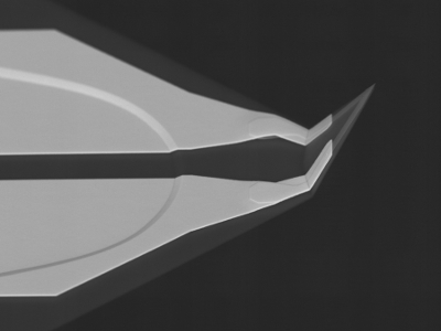
Scanning Thermal Microscopy Probes

KNT-SThM-2an
Unmounted SThM probes for the following methods and applications:
- Combined Thermal and Topographical Imaging
- Temperature Measurement
- Thermal Conductivity Mapping
- Failure Analysis
The Kelvin Nanotechnology KNT-SThM-2an scanning thermal microscopy (SThM) probe is a monolithic, batch fabricated AFM probe for best in class temperature and thermal conductivity mapping, offering excellent flexibility with a standard low spring constant Si3N4 cantilever for easy scanning and high resolution.
Applications
Characterisation of:
- Polymer layers
- Semiconductor & electrical devices
- Biological samples
- Thin films
Pricing
One box of KNT-SThM-2an contains 5 probes:
- UK Price: £1,550 (ex VAT)
- EU Sales: Quotation upon request
- International Sales: Quotation upon request
Please use our contact form or e-mail us for a quotation
Further Information
The tip is manufactured using a multi-layer, direct written electron beam lithography technique developed at the University of Glasgow. Gold pads and tracks connect to a Palladium sensor and heater positioned at the sharp tip apex. Trimming resistors on the probe base adjust the total resistance to fit with most Wheatstone bridge thermal scanning units available from instrument manufacturers. Sub 100 nm topographic and thermal spatial resolution is readily achieved, with a temperature resolution of 0.1 °K
These new SThM probes, based on the existing KNT product KNT-SThM-1an, feature a standard probe base size and a structurally compensated cantilever to give flatter cantilevers and minimise temperature induced cantilever bending. They address a fundamental limitation of soft silicon nitride SThM probes: the thermal bending of the cantilevers when approaching hot surfaces, which ultimately causes the optical feedback to fail. The probes are able to stay in contact with hotter surfaces, expanding the range of measurements and samples that can be employed.

